![]()
Please e-mail comments and suggestions for these guidelines and criteria.
- II. Input/Output
A. Simultaneous Switching Outputs: There are sometimes limits to the number of output pins that can switch at one time; sometimes these are specified by the manufacturer in a data sheet; sometimes it is described in an application note; and sometimes the designer is left on his own. With devices that switch faster and with large pin counts and lower AC and DC noise margins, ground/VDD bounce can be a serious issue. These are a few guidelines to minimize "bounce" issues and items to consider.
- Use low slew outputs unless needed
- Don’t group SSO’s together; break them up (Xilinx: two for each side of a ground pin)
- Control number of SSOs through sequencing Example: Do address and data busses need to switch at the same time?
- For some families, programming “unused” outputs will improve grounding or supply for output stages if terminated to the rail on the printed circuit board.
- Use buffers, particularly for large memory arrays or long lines. Everything does not have to be inside of the FPGA or ASIC.
- Avoid sockets.
- For spare pad locations, pre-wire power, ground, and bypass capacitor connections. “Haywired” power and ground connections will have unneeded inductance.
- Choose input thresholds wisely.
- TTL VIL = 0.8V - very sensitive, try and avoid this setting, as it is sensitive to both ground bounce and ringing.
- Some devices offer programmable 5V CMOS or other input voltage threshold options. This does not reduce ground bounce but mitigates the effects of ground bounce
- Keep clocks physically away from pins that can cause ground bounce.
- Keep clocks close to ground pins
- When Using JTAG and driving board with test data over multiple parts you can induce data pattern sensitivities, particularly with large data busses, perhaps switching patterns from FFFFFFFF Ţ 00000000. This may be an artificial failure, an artifact of the test, but can damage or potentially overstress hardware through a loss of control. JTAG, or the use of reconfigurable components, can be exploited to run ground bounce tests on engineering model and flight hardware.
- Test cabling, particularly for vibration, thermal/vacuum, and EMI tests will present different conditions for normal bench testing or systems application. Design for the worst-case over the entire project flow.
- High-speed parts that are “haywired” in will often have non-optimal connections to the power and ground and poor bypassing. This should be done with care and then properly tested, looking for ground bounce affects.
- For many devices, tPD can be negatively affected by the number of SSOs.
- Ground/VDD bounce can dynamically affect input switching thresholds, decreasing system noise margins.
B. Signal Termination: Ensure that signals are terminated properly.
- Clock signals should need special care to ensure that there is a smooth transition through the threshold. For loaded clocks, perhaps with long runs, reflections may often result in a non-monotonic transitions causing false or double clocking. Note that this may happen on the "inactive" edge. Similarly, overshoot and ringing can also cause false clocking, particularly on the transition to ground.
- Most manufacturers have tight limits on how far outside the rail a signal may travel, sometimes coupled with maximum times outside of the recommended limits. Ensure good signal quality as damage to I/O's may and has happened.
- Do plan on termination resistors in advance. Adding them later is painful, will have lower quality than components and traces located on the circuit board, and will be a major headache for the assemblers.
- Inspect schematics for proper terminations on interfaces such as RS-422, as an example. This is difficult to detect in test as the system may function, to a large extent, without the resistors, although with decreased noise margins and/or increased stress.
C. Tri-State Bus Considerations: Do not allow any overlap in actively driving tri-state busses. This will waste power, needlessly generate noise, and stress components. Have a guaranteed off-time between drivers on the bus in the worst-case. Do not allow the bus to float or have slow transition times, as this will increase power and noise and may negatively affect reliability.
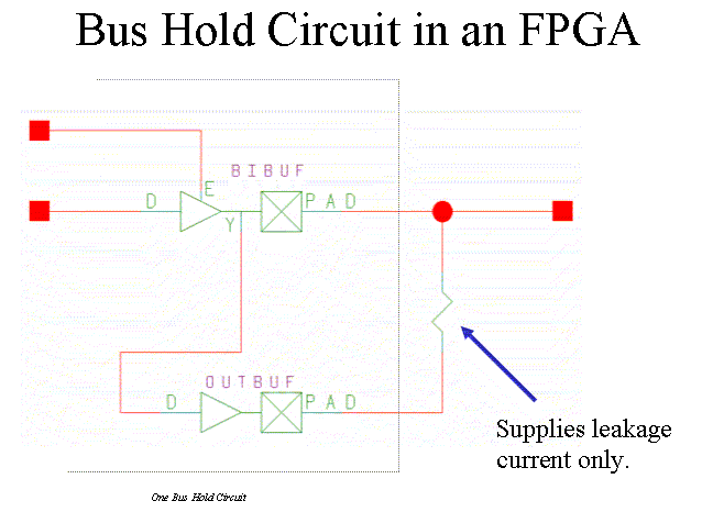
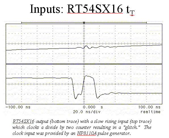
D. Input Transition Times: Some high-speed or modern devices have very stringent restrictions on input transition times, often being surprisingly tight. Failure to meet the requirements may result in oscillations, multiple clocking, or damage. Simple pull-up or pull-down resistors, with transition times in the hundreds of nanoseconds, may often be unacceptable with modern components. In these instances, use bus hold or soft latch circuits, which will also reduce power. In other cases, some older digital logic families may have outputs that are not compatible with modern devices, with the transition times just being too slow.
Waveform measurement is typically from 10% to 90% but not always; sometimes the parameter measurement method is not specified. Care must be taken when protection circuits are used on signals coming onto a board or into a box.
Laboratory tests have shown that not all qualified devices will meet the data sheet. One case was when a part was “shrunk” and there was a migration to a faster process with oscillations observed. Thus, conservative margins are recommended.
E. Shorting Outputs Together: This is sometimes done to increase drive on the board. This should be avoided since it may damage components if the switching speeds are not matched and it can be difficult or impractical to test this redundant topology. If this needs to be done, the two outputs should be from the same integrated circuit and the manufacturer consulted.
F. Pin Assignment: Care and planning is important for pin assignments. First, note the considerations above for simultaneous switching outputs and noise immunity and quiet designs. Take care that clocks and critical signals can be routed on the printed circuit boards for short runs with a minimal of cross-talk, perhaps surrounding it or placing it near to ground pins. Pin assignments that "look pretty" with all the data bits on a bus lined up in a row have been notorious for causing both ground bounce problems on the printed circuit card and routing problems inside FPGAs.
G. Mixed Voltage Interfacing, DC Compatibility. and Noise Margins: When mixing devices from multiple families, even from the same manufacturer, extreme care must be taken to ensure that the devices are reliably operated and that there is sufficient noise margin. This may be problematic when substituting parts for either upgrading circuit performance or dealing with obsolescence issues.
For inputs, many CMOS technology devices advertise "TTL compatible" inputs. However, these inputs may in fact differ rather significantly from their TTL counterparts. The first major difference for many but not all devices is the impedance presented to interface when power is removed for the device. As an example, when radiation-hardened CMOS latches were substituted for SEU-soft 54LS373's in the Galileo attitude control computer's memory units, block redundancy circuits failed since the engineers didn't take into account the sneak path through the inputs ESD protection diodes when power was removed. Another related difference is the maximum voltage that can be applied. Some bipolar devices are useful for reliable level shifting from higher voltages to lower ones; CMOS replacement devices will forward bias the protection diodes resulting in unintended current flows and possible damage or circuit failure. Lastly, many CMOS inputs have logic thresholds which are not truly TTL compatible. That is, the TTL VIH specification is often not met, with VIH(max) values of 2.2V, 2.4V, and sometimes 2.5V being specified whereas true TTL devices have a threshold defined by two diode drops, typically in the range of 1.2V to 1.4V. TTL outputs are only guaranteed to drive to VOH = 2.4V so there may be little or even negative noise margins present in these situation. The switching point difference can also lead to circuit failure, depending on the signal integrity. Often TTL outputs, when switching, have a "bump" in the waveform, particularly with heavy and/or long loads. While this "bump" is often at a high enough voltage so that TTL devices operate correctly, the often higher VIH of CMOS devices may result in multiple clocking. Pull-up resistors can restore adequate DC noise margins in these situations if given enough time to settle, which may be quite a while for this passive circuit. Note, however, that TTL ® CMOS clock interfaces designed in this fashion will often fail since the CMOS input may see multiple transitions resulting in double clocking.
CMOS output stages can also be tricky and subtle device characteristics can cause errors. Check all specifications carefully! For example, many CMOS devices when driving loads are specified at only very low current levels for high or logic '1' signals. However, TTL inputs take substantial currents and do not present the high impedance seen by CMOS FET inputs and the output may be dragged down. For output loads that are a mix of CMOS and TTL inputs, they often must be split to guarantee the high voltage needed for the CMOS inputs, typically 70% of VDD, and the high current needed for TTL inputs, with the lower VIH of 2.0V. Another factor to consider is the structure of the output stage in the CMOS device. For example, some devices will not swing all the way to the high rail and are voltage limited. This may result in some totem-pole current if the p-channel FET in the next input stage is not cut off. Some devices, even with a 5V I/O supply like the RT54SX series, will only drive outputs to the core voltage of 3.3V, making this CMOS output incompatible with 5V CMOS inputs on the same board! This was fixed in the 2.5V core RT54SXS series, with full 5V voltage swings when supplied with a 5V I/O bias.
Components today can typically have many supply voltages of say 1.5V, 1.8V, 2.5, 3.3V, and 5.0V. There are also an abundance of I/O standards with the newest devices being very programmable so their characteristics are not obvious or even knowable from a circuit schematic. Thus, I/O compatibility must be carefully verified, particularly when substituting "new and improved" devices or alternate devices.
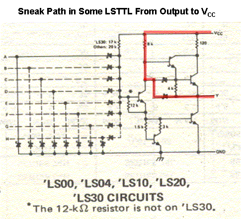
H. Power Switching and Cold Sparing: When designing system with blocks that are independently powered, for either redundancy or power savings mode, considerable care must be taken. Many CMOS devices present a low impedance when powered down through either the intrinsic or ESD protection diodes; others, with cold sparing inputs, may have high input impedance that is suitable for operation. For programmable devices, selecting 3.3V PCI compatibility, as one example, can result in a "cold sparing" device no longer being high impedance since a clamping diode will be enabled. While many bipolar devices are compatible with cold sparing architectures, some devices have a sneak path to VCC through the output.
- "SX-A/RT54SX-S SSO Preliminary Results," October 2, 2002, Actel Corp. sso-10-1-02_actel.pdf
- "Input Transition Times for SX-S FPGAs," OLD News #3, June 24, 2002.
- "Input Transition Times," Section 6 of Programmable Logic Application Notes, November, 2000.
- "Supply-Voltage Migration, 5V to 3.3V." Covers background on processing technologies with implications for supply voltages, distributing multiple supply voltages on a PCB, interfacing between devices operated at different supply voltages, supply voltage sequencing considerations, and migrating designs. xapp080.pdfXL
- "Input Stages," presented at the 2001 MAPLD International Conference, Laurel, MD.
- Typical bus hold circuit. This version exploits the general purpose I/O structure in an FPGA.
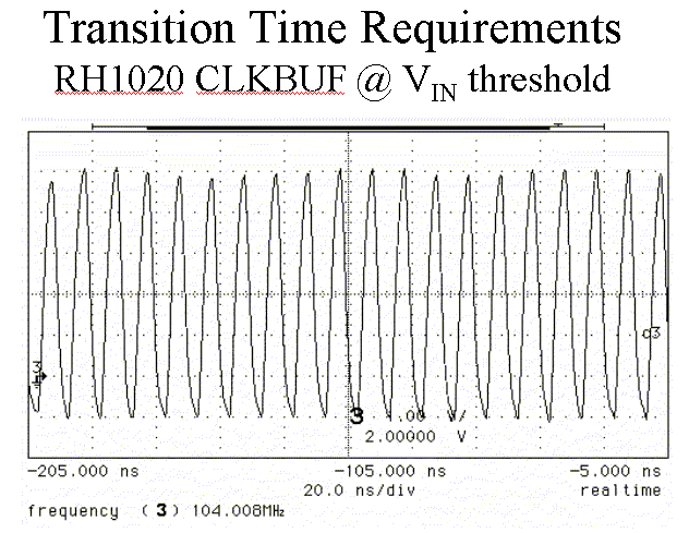
- Slow transition times on the clock input of an RH1020 shows oscillation, although the rise time is less than the specified 500 ns. For this series of tests, the conditions were room temperature and VCC = 5.0 V. Oscillations detected consistently at tR = 360 ns and sporadic output pulses at tR = 300 ns. Note that the transition time performance of the input stages were not symmetric with oscillations detected consistently at tF = 1.5 µs and sporadic output pulses observed at tF = 1.0 µs.
- With the input held at the threshold level, representing the case of a floating input, an RH1020 input stage break's into full oscillation, as seen on the output of the device. For some input stages, the oscillation is not easily seen on the input pin but will propagate within the device.
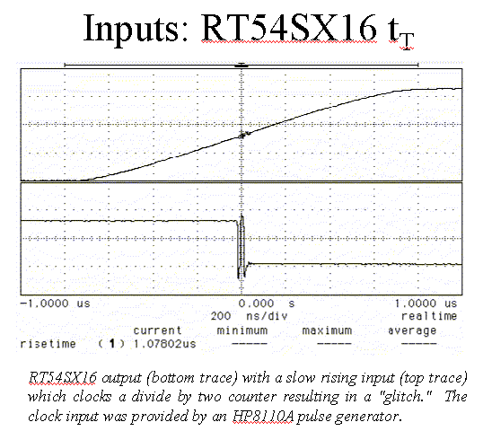
- This example shows the multiple clocking of an RT54SX16 input. A zoomed in view.
- "Signals Into Unpowered CMOS" provides additional discussion.
- "A radiation-hardened cold sparing input/output buffer manufactured on a commercial process line," Benedetto, J.M. Jordan, A., Radiation Effects Data Workshop, 1999, Location: Norfolk, VA. pp. 87-91. Abstract: The radiation hardness of a cold sparing buffer manufactured on a commercial process line is demonstrated. The buffer is shown to be resistant to total dose ionizing radiation and immune (>128 MeV-cm2/mg) to effects from heavy ions such as single event upset (SEU) and single event latch-up (SEL)
- "Input Transition Time," Introduction: Inputs to most CMOS inputs have rise and fall time limitations for reliable operation. Although most if not all programmable logic devices have at least some hysteresis on their inputs, the transition time requirements vary considerably. Below is a table with input transition time requirements for many military and aerospace programmable logic devices.
- The specifications for inputs must be carefully read as not all device or MCM inputs are truly TTL compatible.
- The note "Signal Integrity: IBM Luna C DRAM" gives examples of the requirements for signal integrity, noise levels, and included not only logic signals but the power line. Note that for this device, non-monotonic switching on the control lines may result in unpredictable results.
- "Designing For Signal and Power Integrity in FPGA Systems," Mark Alexander, 2002 MAPLD International Conference, Laurel, MD, September 2002.
- "Drive Strength of Actel FPGAs," Introduction: Many modern CMOS digital microcircuits have very strong drivers; the device characteristics have changed over the years. Another change is the widespread use of HDL synthesis for logic generation and simulators for logic simulation. These simulators do not replace the need to perform proper electrical engineering of spaceborne digital electronics, in particular signal and power integrity.
- "IBIS Models and Simulation," presented at "Design Seminar on Actel SX-A and RTSX-S Programmed Antifuses," Tuesday, April 13, 2004, NASA Goddard Space Flight Center. Review of IBIS and tools along with flight design samples used as case studies.
- "The Effects of Slew Rate on SX-S Series FPGAs," July 18, 2004.
TOP LEVEL: "Design Guidelines and Criteria for Space Flight Digital Electronics"
Home -
NASA Office of Logic Design
Last Revised:
February 03, 2010
Digital Engineering
Institute
Web Grunt: Richard
Katz
